


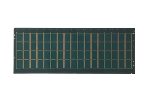
IC Substrates

Ceramic Substrates

High Density PCBs

Packaging Solutions
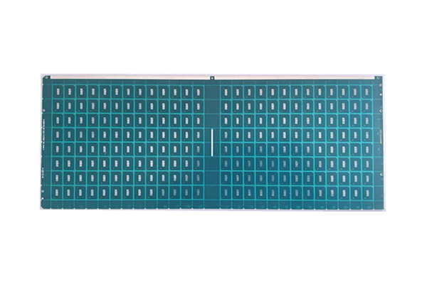
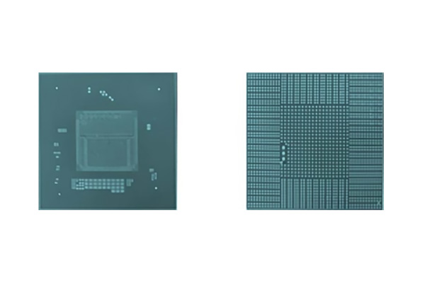
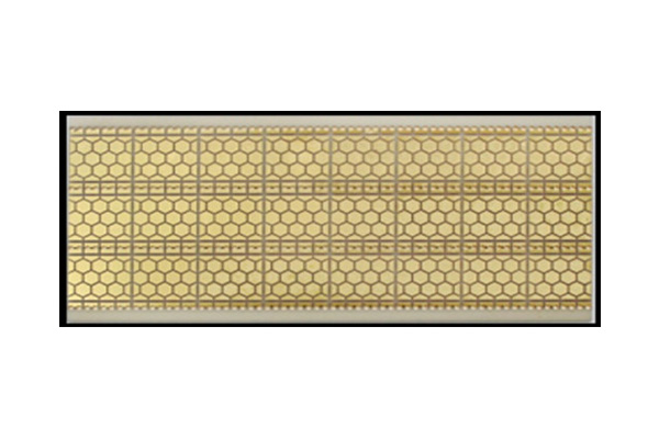
• Application: 800G Optical communication
• Layers: 12L
• Min hole size: 60μm
• Core material: ABF low Dk/Df
• L/S: 15/15μm
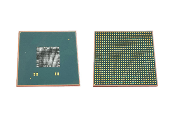
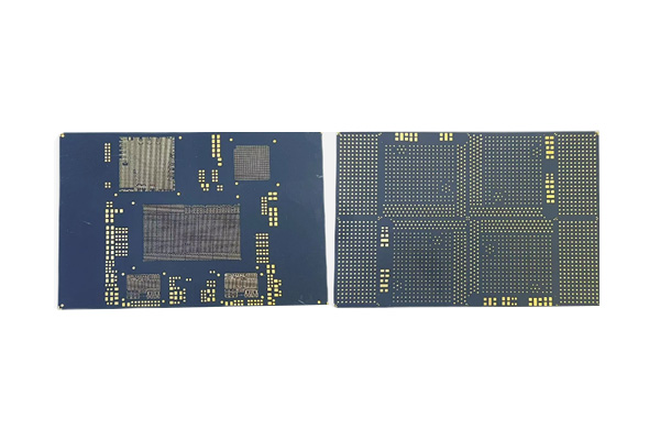
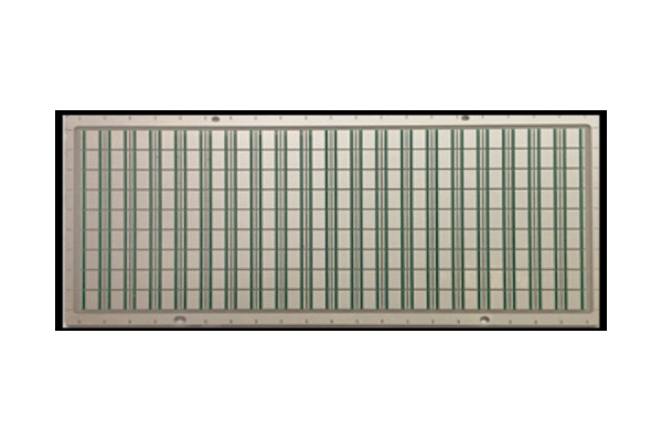
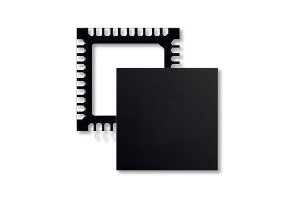
• Application: GPU
• Layers: 10L
• Min hole size: 60μm
• Core material: ABF low Dk/Df
• L/S: 15/15μm
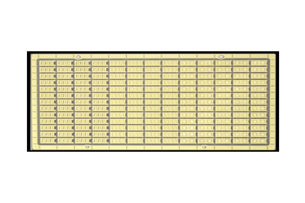
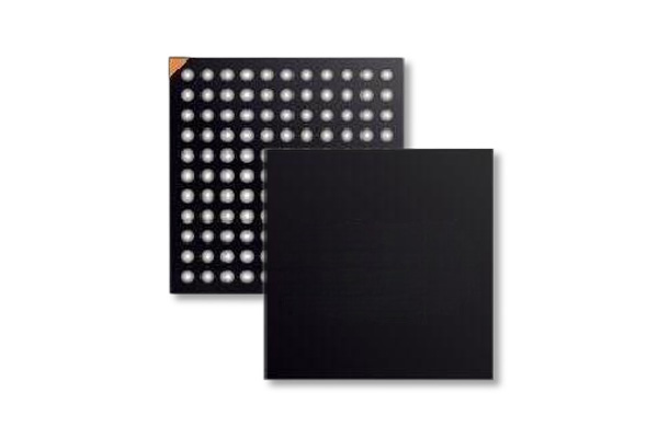
• Product type: FCCSP for memory
• Layers: 4L
• Min. hole size: 80μm
• Core material: ultra low CTE and high TG
• Min. L/S: 20/20μm
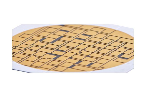
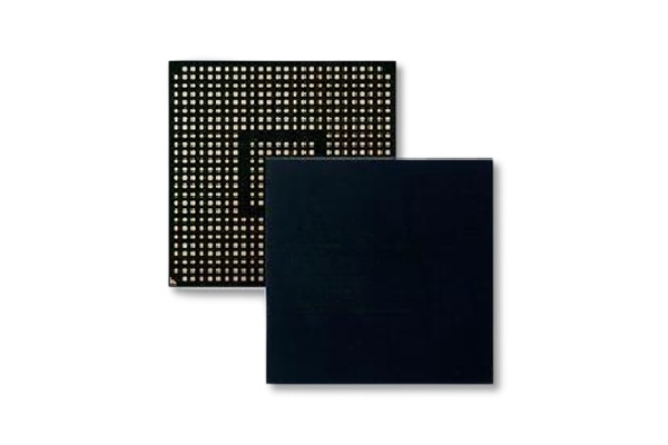
• Product type: FCBGA for CUP
• Layers: 14L
• Min hole size: 60μm
• Core material: ABF+E705G
• Min. L/S: 12/12μm
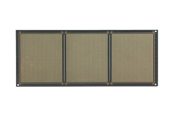
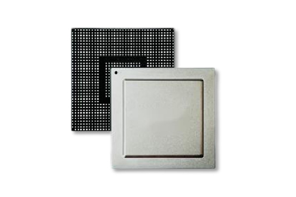
• Application: High performance computing
• Layers: 8L
• Min hole size: 80μm
• Core material: BT low CTE
• L/S: 20/20μm
• Product type: Micro-LED
• Layers: 4L
• Unit size: 8.45x8.45mm
• Core material: HL832NS
• Solder mask: PSR-4000ME
• Min. L/S: 25/25μm
• High thermal conductivity
• Excellent insulation
• Very low coefficient of expansion
• Low dielectric constant and dielectric loss
• Chemical resistance
• High thermal conductivity
• Excellent insulation
• Very low coefficient of expansion
• Low dielectric constant and dielectric loss
• Chemical resistance
• Ultra-high thermal conductivity (170-220W/m.K)
• Excellent insulation
• Extremely low expansion coefficient
• Low dielectric constant and dielectric loss
• Resistance to chemical corrosion
• High thermal conductivity
• Excellent insulation
• Very low coefficient of expansion
• Low dielectric constant and dielectric loss
• Chemical resistance
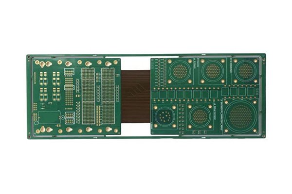
• 14L, rigid-flex
• Air Gap design
• applied in the field of
• large medical equipment
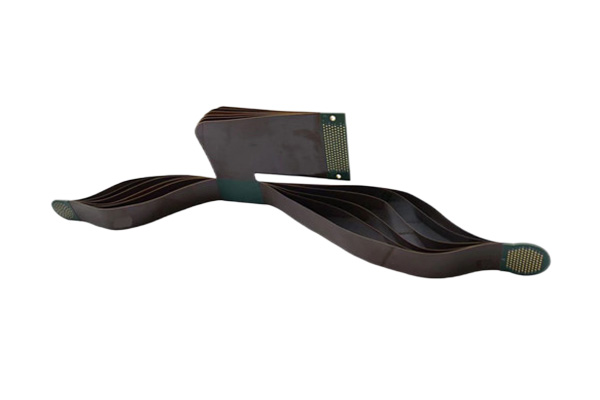
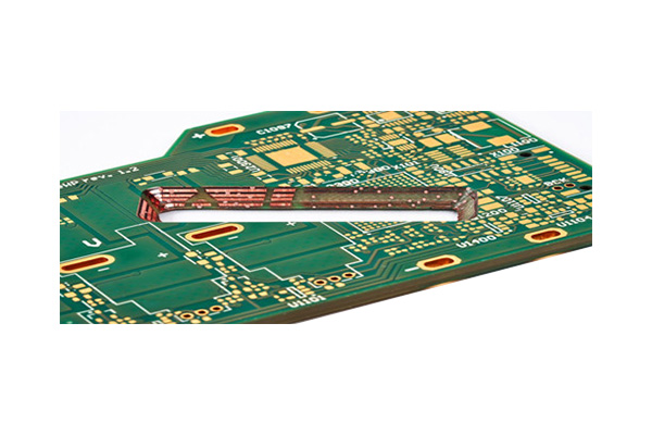
• 18L rigid-flex
• 2(rigid)+14(flex)+2(rigid)
• Air Gap design
• Applied in the field of high-end communication
• The base copper can reach 3OZ
• And the finished copper thickness can reach 12OZ
• It is widely used in microwave, aerospace
• Satellite communication
• Network base station
• Hybrid integrated circuit
• Power high-power circuit and other high-tech fields
• Up to 32 layers
• And the structure can realize any layer interconnection
• Which is widely used in mobile phones
• Digital cameras, notebook
• Automotive electronics and other digital products
• Small in size and light in weight
• Low power consumption
• Good heat dissipation effect
• High system integration
• Low production cost and short market launch cycle
• Small in size and light in weight
• Good heat dissipation performance
• Excellent electrical performance
• Lower cost
• High reliability
• High-density HDI fine pitch substrate
• Advanced bonding process
• Mature technology and low cost
• High wiring density
• Support for multi-chip applications
• Support antenna applications within the package
• High reliability
• High-density interconnection
• Excellent heat dissipation performance
• Low inductance and resistance
• High reliability
• Miniaturized design
Reach out to us via chat, phone, or our simple contact form.
Get a FREE Quote Today
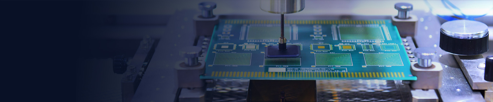
Circuit-Chip provides advanced semiconductor substrates, packaging and engineering support for high-performance electronic applications. Our capabilities cover IC substrate design and fabrication, advanced packaging, simulation, testing, reliability support and selected high-density interconnect solutions for applications such as optical communication, AI computing, RF and industrial electronics.