


• Up to 32 layers
• And the structure can realize any layer interconnection
• Which is widely used in mobile phones
• Digital cameras, notebook
• Automotive electronics and other digital products
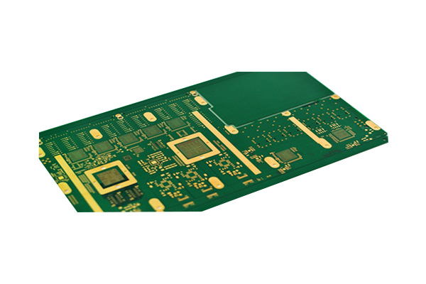
Multilayers HDI (High-density Interconnect Multilayer Board) is an advanced printed circuit board (PCB) technology in the field of modern electronic manufacturing. It combines the high-density routing capability of multilayers and the high-precision interconnect characteristics of HDI technology, and is widely used in electronic products with extremely high requirements for circuit performance and space utilization.
Technical characteristics
High-density cabling: Through multi-layer stacking and micro-hole techniques (such as laser drilling), finer wire widths/wire spacings (typically less than 75μm) and smaller hole diameters (typically less than 150μm) are achieved, significantly enhancing the cabling density.
Multi-layer structure: It usually contains more than 4 layers, and can even reach 20 or more layers. Through lamination processes, multiple conductive and insulating layers are alternately stacked to achieve complex circuit functions.
Micro-hole interconnection: By adopting various interconnection methods such as Blind Via, Buried Via and Through Via, the signal transmission path is optimized and signal interference is reduced.
Thin dielectric layer: The thickness of the dielectric between layers is usually between 50μm and 100μm, further reducing the size of the circuit board and improving space utilization.
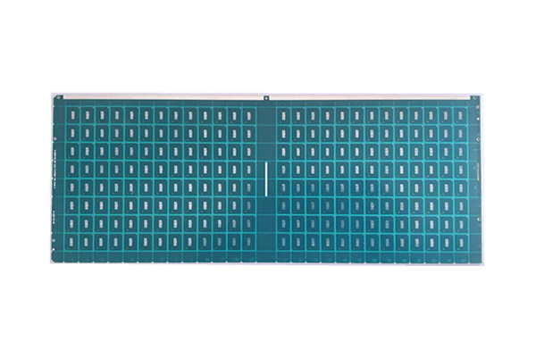
• Application: 800G Optical communication
• Layers: 12L
• Min hole size: 60μm
• Core material: ABF low Dk/Df
• L/S: 15/15μm
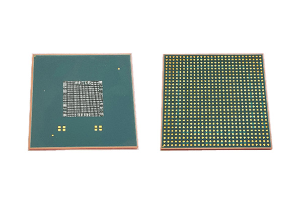
• Application: GPU
• Layers: 10L
• Min hole size: 60μm
• Core material: ABF low Dk/Df
• L/S: 15/15μm
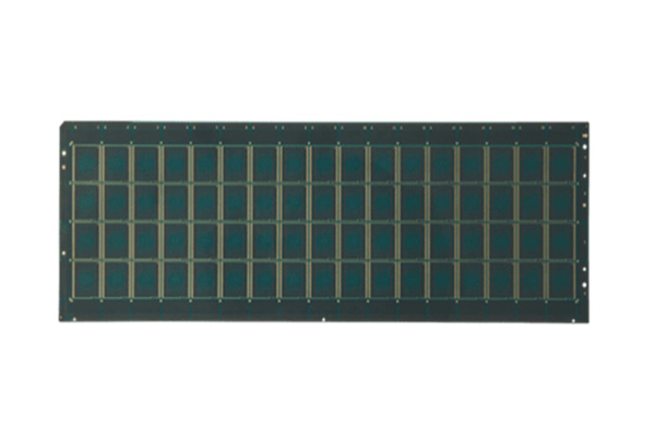
• Product type: FCCSP for memory
• Layers: 4L
• Min. hole size: 80μm
• Core material: ultra low CTE and high TG
• Min. L/S: 20/20μm
Reach out to us via chat, phone, or our simple contact form.
Get a FREE Quote Today
Circuit-Chip provides advanced semiconductor substrates, packaging and engineering support for high-performance electronic applications. Our capabilities cover IC substrate design and fabrication, advanced packaging, simulation, testing, reliability support and selected high-density interconnect solutions for applications such as optical communication, AI computing, RF and industrial electronics.