


• Small in size and light in weight
• Good heat dissipation performance
• Excellent electrical performance
• Lower cost
• High reliability
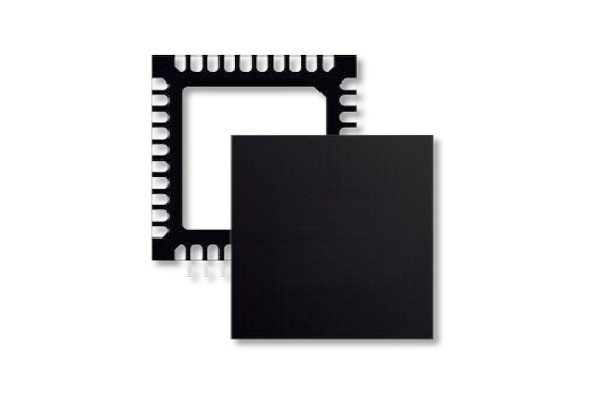
QFN (Quad Flat No-lead Package), namely square flat no-lead package, is a technology widely used in the field of integrated circuit packaging. The following is an introduction from aspects such as definition, structural characteristics, advantages, application fields, technical challenges and development directions:
Structural characteristics
Pin-free design: The four sides of the package are equipped with electrode contacts, but there are no external pins. This results in a smaller surface mount area than QFP (four-sided pin flat package) and a lower height than QFP. However, when stress occurs between the printed substrate and the package, it cannot be relieved at the electrode contact points. Therefore, the number of electrode contacts is generally around 14 to 100, which is less than that of the QFP package.
Bottom pad: At the center of the bottom of the package, there is a large exposed pad for heat conduction. Around the periphery of the package that surrounds the large pad, there are conductive pads for electrical connection.
The materials are diverse: There are two types of materials, namely ceramic and plastic. When there is an LCC mark, it is basically ceramic QFN. Plastic QFN is a low-cost package based on a glass epoxy resin printed substrate. Besides 1.27mm, the center distance of the electrode contacts also comes in two types: 0.65mm and 0.5mm.
• Application: 800G Optical communication
• Layers: 12L
• Min hole size: 60μm
• Core material: ABF low Dk/Df
• L/S: 15/15μm
• Application: GPU
• Layers: 10L
• Min hole size: 60μm
• Core material: ABF low Dk/Df
• L/S: 15/15μm
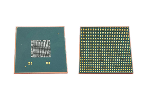
• Product type: FCCSP for memory
• Layers: 4L
• Min. hole size: 80μm
• Core material: ultra low CTE and high TG
• Min. L/S: 20/20μm
Reach out to us via chat, phone, or our simple contact form.
Get a FREE Quote Today
Circuit-Chip provides advanced semiconductor substrates, packaging and engineering support for high-performance electronic applications. Our capabilities cover IC substrate design and fabrication, advanced packaging, simulation, testing, reliability support and selected high-density interconnect solutions for applications such as optical communication, AI computing, RF and industrial electronics.