


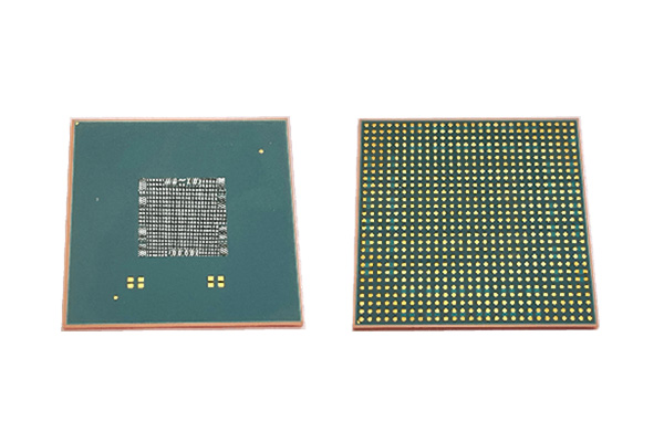
• Product type: FCCSP for memory
• Layers: 4L
• Min. hole size: 80μm
• Core material: ultra low CTE and high TG
• Min. L/S: 20/20μm
CSP (Chip Scale Package), namely chip-level packaging, is an integrated circuit packaging solution dedicated to achieving ultra-small volume and high integration. The following is an introduction from multiple aspects:
Technical principle: The core principle of CSP packaging is to optimize the packaging structure and process to make the size of the packaged device as close as possible to the size of the chip itself, while meeting multiple requirements such as electrical connection, heat dissipation, and mechanical protection. By reconfiguring the connection mode between the chip and the outside world, it enables the package body to actively approach the Die Size, significantly reducing the PCB area occupied by the package.
Features:
Ultimate miniaturization: CSP packaging enables the ratio of chip area to packaging area to exceed 1:1.14, and its absolute size is only about 32 square millimeters, approximately one-third the size of a regular BGA and one-sixth the size of a TSOP memory chip.
High integration: Among various packages of the same size, the number of input/output terminals for CSP can be greater. For example, for a 40mm×40mm package, the maximum number of input/output terminals for QFP is 304, for BGA it can reach 600 to 700, and for CSP it is very easy to reach 1000.
Superior performance: The length of the interconnection lines between the chips inside the CSP and the packaging shell wiring is much shorter than that of QFP or BGA, thus resulting in smaller parasitic parameters and shorter signal transmission delay time, which is conducive to improving the high-frequency performance of the circuit. Meanwhile, the electrical performance and reliability of CSP packaging have also been significantly improved compared to BGA and TSOP.
Excellent heat dissipation performance: Most CSPS install the chip facing down, which can dissipate heat from the back of the chip, and the effect is good. The thermal resistance of CSP is relatively low. For instance, the thermal resistance of CSP is 35℃/W, while that of TSOP is 40℃/W.
Compatible with SMT processes: Pin pitch (0.5~1mm), suitable for existing surface mount equipment, allowing for mass production without the need to modify the production line.
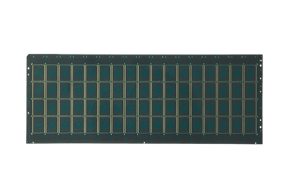
• Application: 800G Optical communication
• Layers: 12L
• Min hole size: 60μm
• Core material: ABF low Dk/Df
• L/S: 15/15μm
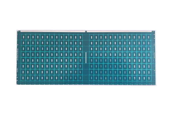
• Application: GPU
• Layers: 10L
• Min hole size: 60μm
• Core material: ABF low Dk/Df
• L/S: 15/15μm
• Product type: FCCSP for memory
• Layers: 4L
• Min. hole size: 80μm
• Core material: ultra low CTE and high TG
• Min. L/S: 20/20μm
Reach out to us via chat, phone, or our simple contact form.
Get a FREE Quote Today
Circuit-Chip provides advanced semiconductor substrates, packaging and engineering support for high-performance electronic applications. Our capabilities cover IC substrate design and fabrication, advanced packaging, simulation, testing, reliability support and selected high-density interconnect solutions for applications such as optical communication, AI computing, RF and industrial electronics.