


• Small in size and light in weight
• Low power consumption
• Good heat dissipation effect
• High system integration
• Low production cost and short market launch cycle
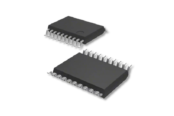
The SOP (Small Outline Package) chip is a common form of surface mount integrated circuit packaging. The following is an introduction from aspects such as packaging structure, technical characteristics, application fields, variant types, and test requirements:
Packaging structure
Pin distribution: The pins of the SOP chip are distributed on both sides of the chip, presenting a seagull wing shape (L-shaped) or J-shaped (SOJ package).
Encapsulation material: Plastic is usually used as the encapsulation material, and sometimes ceramic is also used.
Package height: The package height is as low as 1.75mm, compact in size and light in weight.
Technical characteristics
Pin count and pitch: The pin count is generally between 8 and 64, and the pin pitch is usually 0.65mm, 0.8mm or 1.27mm.
High integration: SOP packaging can achieve the integration of high-Q circuits and high-power modules through multi-layer three-dimensional structures such as LTCC process, and the system integration is high.
Low cost: Due to the mature packaging process, the production cost is relatively low.
Excellent electrical performance: It has excellent thermal and electrical performance and supports the installation of high-density circuit boards.
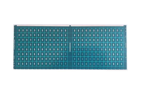
• Application: 800G Optical communication
• Layers: 12L
• Min hole size: 60μm
• Core material: ABF low Dk/Df
• L/S: 15/15μm
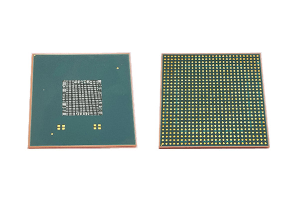
• Application: GPU
• Layers: 10L
• Min hole size: 60μm
• Core material: ABF low Dk/Df
• L/S: 15/15μm
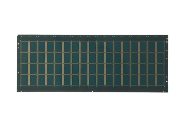
• Product type: FCCSP for memory
• Layers: 4L
• Min. hole size: 80μm
• Core material: ultra low CTE and high TG
• Min. L/S: 20/20μm
Reach out to us via chat, phone, or our simple contact form.
Get a FREE Quote Today
Circuit-Chip provides advanced semiconductor substrates, packaging and engineering support for high-performance electronic applications. Our capabilities cover IC substrate design and fabrication, advanced packaging, simulation, testing, reliability support and selected high-density interconnect solutions for applications such as optical communication, AI computing, RF and industrial electronics.