


• High wiring density
• Support for multi-chip applications
• Support antenna applications within the package
• High reliability
FCCSP (Flip Chip Chip Scale Package) is an advanced microelectronic packaging technology and has the following characteristics:
Small package size The packaging size of FCCSP is almost close to the size of the bare chip. Generally, the ratio of the chip area to the packaging area is approximately 1:1.1. According to the JSTK-012 standard of JEDEC, products with a chip packaging area less than or equal to 120% of the LSI chip area are called CSP. This is also the basis of FCCSP. This miniaturized design gives it a significant advantage in electronic devices with strict space requirements. For instance, in mobile devices such as smart phones and tablet computers, it can effectively save space and meet the design requirements of thin and light products.
High wiring density: It can provide higher wiring density, lower inductance and shorter signal path. Due to the short signal path, the loss and interference of the electrical signal during transmission are relatively small, thereby optimizing the electrical performance. This makes FCCSP not only suitable for low-frequency applications but also perform well in high-frequency applications. For example, in the baseband chips or RF chips of communication equipment, the adoption of FCCSP packaging can ensure the rapid and stable transmission of signals and improve the communication quality.
Support for multi-chip applications: It supports multi-chip (side-by-side stacking) applications, achieving higher integration and functionality. By integrating multiple chips into one package, more functions can be achieved in a smaller space. For instance, in some complex artificial intelligence chips or neural network chips, chips with different functions can be stacked and packaged to enhance the overall performance and functional diversity of the chips.
• Application: 800G Optical communication
• Layers: 12L
• Min hole size: 60μm
• Core material: ABF low Dk/Df
• L/S: 15/15μm
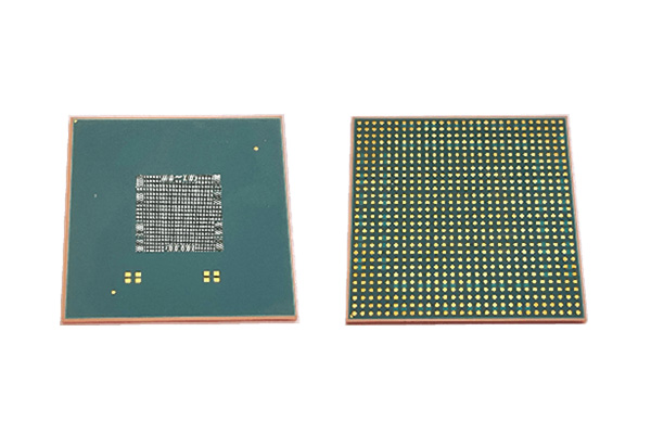
• Application: GPU
• Layers: 10L
• Min hole size: 60μm
• Core material: ABF low Dk/Df
• L/S: 15/15μm
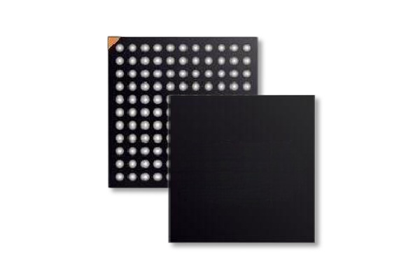
• Product type: FCCSP for memory
• Layers: 4L
• Min. hole size: 80μm
• Core material: ultra low CTE and high TG
• Min. L/S: 20/20μm
Reach out to us via chat, phone, or our simple contact form.
Get a FREE Quote Today
Circuit-Chip provides advanced semiconductor substrates, packaging and engineering support for high-performance electronic applications. Our capabilities cover IC substrate design and fabrication, advanced packaging, simulation, testing, reliability support and selected high-density interconnect solutions for applications such as optical communication, AI computing, RF and industrial electronics.