

• The base copper can reach 3OZ
• And the finished copper thickness can reach 12OZ
• It is widely used in microwave, aerospace
• Satellite communication
• Network base station
• Hybrid integrated circuit
• Power high-power circuit and other high-tech fields
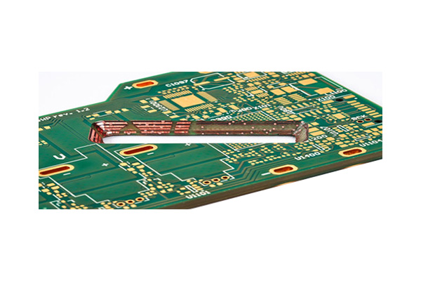
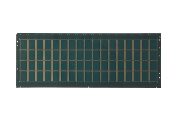
Heavy Copper (thick copper board) is a special printed circuit board (PCB) used to carry large currents and high power. Its copper layer thickness is significantly higher than that of conventional PCBS. Usually, the outer copper thickness is between 2 and 20 ounces (oz) (about 70 to 700 microns), and the inner copper thickness can even be superimposed to a higher level.
Definition and Classification of copper thickness
Copper thickness range:
Outer copper thickness: 2-20oz (70-700μm)
Inner copper thickness: Can be superimposed to a higher level (such as 200oz)
Classification basis:
Even if the total Copper content is less than 3oz, if the thickness of a single layer of copper exceeds 4oz per square foot, it is still classified as a Heavy Copper PCB.
Core characteristics
High current carrying capacity: Supports large currents of over 100A, suitable for high-power devices.
Excellent heat dissipation performance: Direct heat conduction through the copper layer (such as welding the heat sink of the TO-220 package TO the copper surface) enhances thermal stability.
Resistance to thermal cycling and corrosion: It can operate stably for a long time in high-temperature (such as welding heat) and corrosive environments.
High electrical connection strength: Provides stronger electrical connection points to reduce signal interference.
• Application: 800G Optical communication
• Layers: 12L
• Min hole size: 60μm
• Core material: ABF low Dk/Df
• L/S: 15/15μm
• Application: GPU
• Layers: 10L
• Min hole size: 60μm
• Core material: ABF low Dk/Df
• L/S: 15/15μm
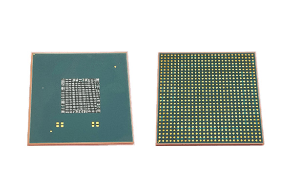
• Product type: FCCSP for memory
• Layers: 4L
• Min. hole size: 80μm
• Core material: ultra low CTE and high TG
• Min. L/S: 20/20μm
Reach out to us via chat, phone, or our simple contact form.
Get a FREE Quote Today
Circuit-Chip provides advanced semiconductor substrates, packaging and engineering support for high-performance electronic applications. Our capabilities cover IC substrate design and fabrication, advanced packaging, simulation, testing, reliability support and selected high-density interconnect solutions for applications such as optical communication, AI computing, RF and industrial electronics.