


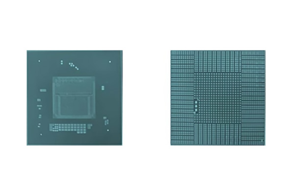
• Product type: FCBGA for CUP
• Layers: 14L
• Min hole size: 60μm
• Core material: ABF+E705G
• Min. L/S: 12/12μm
FCBGA packaging adopts flip-chip technology, that is, the circuit surface of the chip faces down and is directly electrically connected to the packaging substrate through solder balls. Unlike traditional wire-bonded packaging, FCBGA packaging eliminates the leads between the chip and the substrate, significantly shortening the signal transmission path and enhancing the signal transmission speed and reliability.
Structural characteristics
Chip flip-chip: The circuit surface of the chip faces down and is connected to the substrate through solder balls, reducing the delay and loss of signal transmission.
Ball grid array: At the bottom of the packaging substrate, there are a large number of regularly arranged solder balls. These solder balls serve as electrical connection points between the chip and external circuits, providing high-density I/O interfaces.
Packaging substrate: The packaging substrate serves to support the chip, electrical connections, and heat dissipation, etc. It typically adopts a multi-layer wiring structure to meet the complex electrical connection requirements between the chip and external circuits.
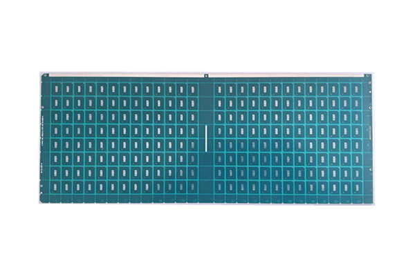
• Application: 800G Optical communication
• Layers: 12L
• Min hole size: 60μm
• Core material: ABF low Dk/Df
• L/S: 15/15μm
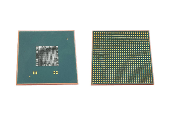
• Application: GPU
• Layers: 10L
• Min hole size: 60μm
• Core material: ABF low Dk/Df
• L/S: 15/15μm
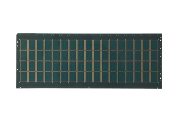
• Product type: FCCSP for memory
• Layers: 4L
• Min. hole size: 80μm
• Core material: ultra low CTE and high TG
• Min. L/S: 20/20μm
Reach out to us via chat, phone, or our simple contact form.
Get a FREE Quote Today
Circuit-Chip provides advanced semiconductor substrates, packaging and engineering support for high-performance electronic applications. Our capabilities cover IC substrate design and fabrication, advanced packaging, simulation, testing, reliability support and selected high-density interconnect solutions for applications such as optical communication, AI computing, RF and industrial electronics.