


LG Innotek Unveils Copper Post Technology for Smaller, Cooler RF-SiP Substrates
Jul 10,2025
June 25, 2025,LG Innotek (KRX: 011070) has announced the successful development of the world’s first Copper Post (Cu-Post) technology for semiconductor substrates—a significant innovation in advanced chip packaging, especially for RF system-in-package (RF-SiP) solutions used in mobile and AI-powered devices.
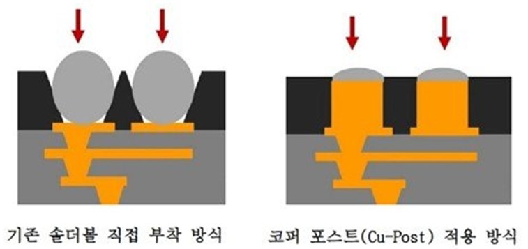
Traditionally, solder balls have served as the interconnection method between semiconductor chips and substrates. LG Innotek’s Cu-Post technology replaces these solder balls with ultra-fine copper pillars, achieving up to a 20% reduction in substrate footprint while maintaining—or even improving—electrical performance and reliability.
“Cu-Post is a game-changer for space-constrained, high-performance applications,” stated a company spokesperson. “It enables tighter circuit pitches and superior heat dissipation, which are critical for next-generation smartphones and AI hardware.”
Key Benefits of Cu-Post Technology:
20% Smaller Substrate Size
Higher Signal Density and Integration
Superior Thermal Conductivity (copper offers ~7x better heat dissipation than traditional solder)
Ready for Production in RF-SiP and Flex PCBs
With the surge in demand for compact, thermally efficient, and high-speed chip packaging, this innovation positions LG Innotek as a leader in the evolving substrate packaging landscape. The company plans to apply Cu-Post technology to a wide range of devices, starting with mobile RF modules and potentially expanding to high-performance computing (HPC) sectors.
While distinct from glass substrate technologies under development by Intel and Samsung, Cu-Post shares the same goal—enabling smaller, faster, and more efficient semiconductor packages. Unlike glass substrates, which remain in the early commercialization stage, Cu-Post is production-ready and compatible with existing RF-SiP and flexible PCB processes.
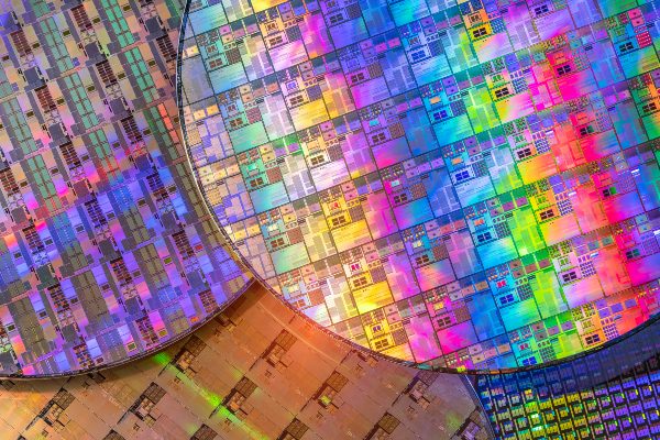
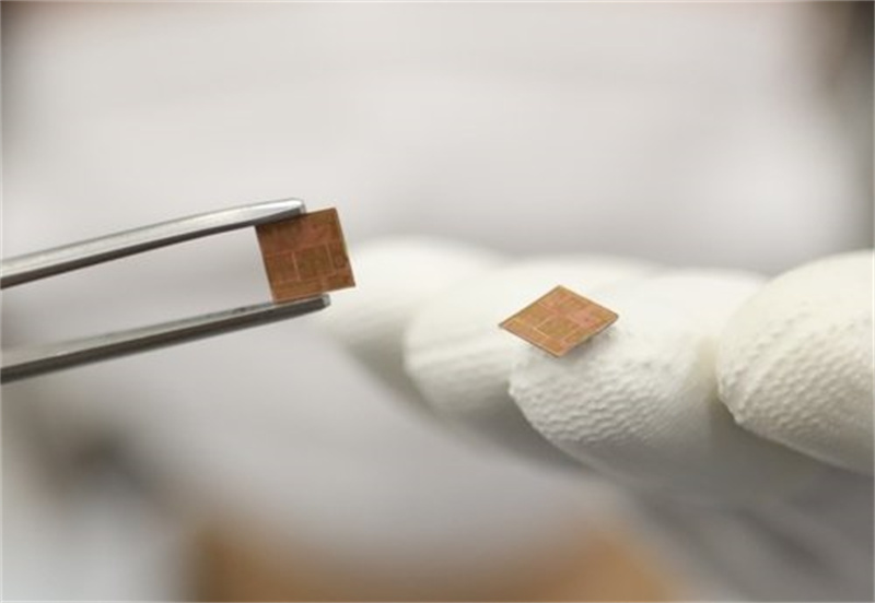
Copper Post (Cu-Post) sample image, courtesy of LG Innotek.
This milestone highlights LG Innotek’s ongoing commitment to pushing the boundaries of semiconductor substrate technology, as the industry accelerates toward miniaturized, high-performance, and thermally optimized packaging solutions.