


Vietnam to Launch $69M Semiconductor Packaging Lab in Da Nang by 2026
Jul 29,2025
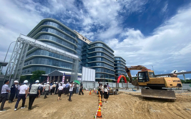
Da Nang, Vietnam – July 28, 2025 – Vietnam’s Ministry of Science and Technology, in partnership with the Da Nang People’s Committee, has officially kicked off construction of the Advanced Packaging Technology Manufacturing Laboratory (Fab-Lab). The new facility will be located within Da Nang Software Park No. 2, marking a major leap in the country’s efforts to develop a domestic semiconductor packaging ecosystem.
With a total investment of VND 1.8 trillion (approximately $68.8 million USD), the Fab-Lab is being positioned as a pioneering model for advanced packaging research and pilot production in Vietnam. The project covers a 2,288-square-meter site and will offer more than 5,700 square meters of usable floor space, divided into two core zones:
Lab Zone: R&D for Next-Gen Packaging
This area will be dedicated to research and development of cutting-edge packaging technologies including:
Fan-Out Wafer Level Packaging (FOWLP)
2.5D/3D Integrated Circuits (ICs)
Silicon Interposers
Silicon Bridge Packaging Technologies
These technologies are essential for supporting high-performance computing (HPC), AI chips, and space-constrained mobile or automotive applications.
Fab Zone: Pilot Production for Real Wafers
The second zone will focus on pilot-scale semiconductor packaging, with facilities to handle real wafers using state-of-the-art equipment, including:
Photolithography systems
Wafer bonding machines
Precision metrology and testing tools compliant with international standards
Designed Capacity & Timeline
Annual Capacity: Up to 10 million units
Target Markets: Domestic and international customers
Operational Launch: Expected in Q4 2026
Once operational, the Fab-Lab will serve as both a national research hub and a semiconductor manufacturing incubator, supporting Vietnamese firms and foreign partners looking to explore or scale up advanced packaging solutions in Southeast Asia.