TSMC Accelerates Development of CoPoS Packaging Technology to Meet AI Chip Demand
Jun 12,2025
Taiwan Semiconductor Manufacturing Company (TSMC) is advancing its next-generation advanced packaging technology, CoPoS (Chip-on-Panel-on-Substrate), in response to growing demand for AI-centric chip solutions. According to reports from MoneyDJ and the Economic Daily News on June 11, TSMC plans to establish its first CoPoS pilot line in 2026, with mass production slated to begin between late 2028 and early 2029. NVIDIA is expected to be the first major customer.
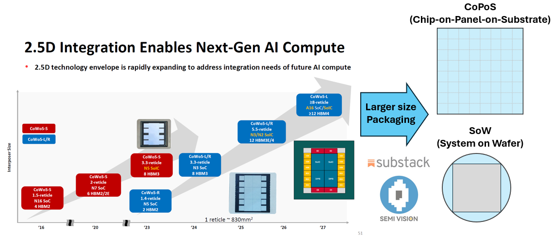
CoPoS represents a strategic evolution of TSMC's existing CoWoS-L and CoWoS-R technologies. Unlike traditional round wafers, CoPoS uses large square panels—measuring 310mm by 310mm—as the substrate. This format offers significantly greater usable area, improving substrate efficiency, reducing cost per unit, and enabling more flexible chip integration for high-performance applications such as AI, HPC, and 5G.
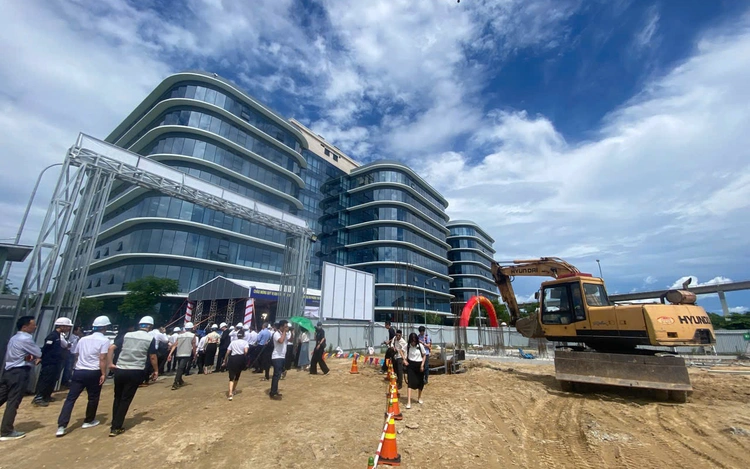
The CoPoS project will be housed at TSMC's AP7 site in Chiayi, which is currently under phased development. Phase 1 of AP7 will focus on WMCM (multi-chip module) production for Apple, while Phases 2 and 3 will ramp up TSMC's SoIC production. Phase 4 will be dedicated to large-scale CoPoS manufacturing. TSMC's existing CoWoS production, meanwhile, will remain at its AP8 facility, formerly an Innolux plant.
TSMC will initially build a CoPoS trial line at the facilities of its subsidiary Xintec, leveraging the site's legacy in optics and its experience in panel-level packaging. Trial production is expected in late 2026 to early 2027, followed by technology development in 2027 and process validation in 2028 ahead of volume ramp-up.
CoPoS is expected to primarily serve AI-related chip needs, with NVIDIA leading adoption, followed by AMD and Broadcom. The platform's design advantages—including higher yield per panel and compatibility with larger form factors—are seen as critical in meeting the compute demands of next-gen AI and HPC workloads.
As the semiconductor industry pushes toward greater integration and performance, CoPoS could become a defining platform in the evolution of advanced packaging—merging the scalability of fan-out panel-level packaging (FOPLP) with the proven high-density interconnects of CoWoS.
TSMC's shift from round wafers to panel-based substrates marks a pivotal move in the chip packaging landscape, with implications for efficiency, cost, and AI-era scalability.


